


Allion Labs
What is SMT (Surface Mount Technology)?
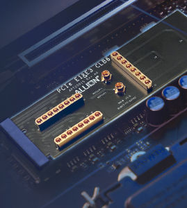
Surface Mount Technology (SMT) is one of the most popular techniques and processes in the electronic assembly industry. The Surface Mount Assembly (SMA) technique is a surface mounting or installation method that mounts the leadless or short-lead surface mount components (SMC, also known as SMD, surface mount device) on the surface of the printed circuit board (PCB) or other base plates. It is a circuit mounting technique that uses reflow soldering or dip soldering to solder the components.
What are the basic processes of SMT?
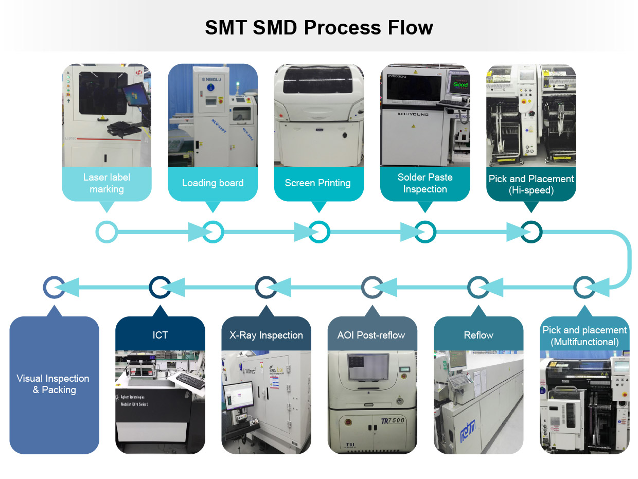
The basic processes of SMT are as the following: screen print comes first, which will allow the following glue dispensing, mounting, reflow soldering, cleaning, SPI, inspection, and defect rework.
- Screen print: A preparatory work for the soldering of the components, which prints the soldering paste or glue patch on the PCB pads. It requires the screen printer (screen printing machine) that is located at the foremost end of the SMT production line.
- Glue dispensing: The glue is dispensed at fixed locations on the PCB. The main purpose of the glue is to fixture the components on the PCB. It requires the glue dispenser that is located at the foremost end or after the inspection equipment in the SMT production line.
- Mounting: This is to precisely install the surface mounting components on fixed locations of the PCB. It requires the mounting machine that is located after the screen printer in the production line.
- Reflow soldering: During this process, the soldering paste is melted, enabling the surface mounting components to be strongly glued together with the PCB. It requires a curing furnace that is located at the rear side of the mounting machine in the production line.
- Cleaning: In this process, the soldering residues that are harmful to the human body on the assembled PCB, such as the flux, are removed. It requires a cleaning machine and its location can vary, whether within or out of the production line.
- Solder paste inspection (SPI): In this process, the bad volume, area, height, offset, defects, damages, height deviation, etc. of solder paste printing are detected.
- Inspection: This process reviews the soldering quality and assembly quality of the assembled PCB. It requires a magnifier, microscope, in-circuit tester (ICT), flying probe tester (FPT), automatic optical inspection (AOI), x-ray inspection system, functional tester, etc., which can be allocated at an adequate location in the production line based on the inspection requirements.
- Rework: After the inspection, the PCBs detected with malfunctions are reworked. The necessary tools are soldering iron, rework station, etc., which can be allocated at any location in the production line.
Based on the location of the assembled component, it can be divided into two types: single-sided boards and double-sided boards.
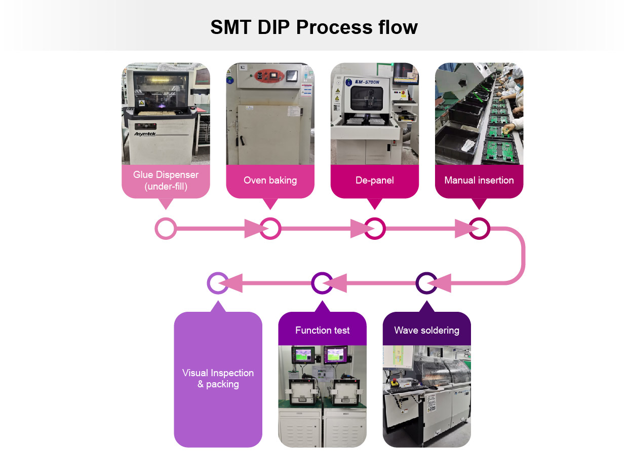
- Production flow of a single sided board
PCB placement → Laser engraving SN → Soldering paste applied with screen print → SPI → Mounting → AOI → Reflow soldering → Board cutting → Inspection → Defect reworking
- Production flow of a double sided board
PCB placement → Laser engraving SN → Soldering paste applied on side A with screen print → SPI → Mounting → AOI → Reflow soldering of side A→ Turning the board → Soldering paste applied on side B with screen print → SPI → Mounting → AOI → Reflow soldering → Board cutting → Inspection → Defect reworking
Understand the SMT production flow
AOI (Automatic Optical Inspection)
AOI and ICT are the common types of circuit board inspections in the industry, and they are complementary to each other. Here’s a quick introduction for both of them.
The automatic optical inspection system is now commonly applied in the appearance inspection of the circuit board assembly production lines in the electronic industry, replacing the visual inspection approach of the past.
The basic principle of AOI
Powered by image technology, the object to be inspected and a standard image are compared for their difference to determine whether the object to be inspected meets the criteria. Thus, the quality of the AOI result heavily relies on factors including image resolution, image formation, and image recognition technology.
It is used to detect the quality of the circuit board parts after PCB assembly on the SMT assembly line. or to determine whether the soldering paste printing meets the criteria.
The greatest advantage of AOI
It can replace the traditional manual inspections required both before and after the SMT oven process. Also, it is more accurate than human vision when determining the defects of the SMT’s assembly.
The greatest disadvantage of AOI
“False reject” may occur in places with grayish colors or unclear shadows. Part of such circumstances can be resolved when supported with lights of different colors, yet the inspection for components covered by other parts or solder joints beneath certain components remains the biggest problem. Traditional AOI can only inspect places under direct light; however, components blocked by the frames or beneath the borders are usually missed by AOI inspection.
Thus, AOI is rarely the only process used for the quality assurance of general circuit board assembly lines, as ICT (in-circuit test) and FVT applications are still required for effective inspections, even an automatic x-ray inspection process may be added in some cases, where x-ray is used to check the quality of the solder joints (e.g., BGA) under the components along the lines, guaranteeing 100% inspection coverage on the circuit board.
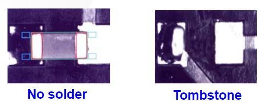
AOI can detect the following defects of the assembled circuit board:
- Missing
- Skew
- Tombstone
- Wrong component
- Wrong polarity
- Lead lift and lead defective
- Solder bridge
- Insufficient solder
- Non-wetting and cold soldering
ICT (In-Circuit-Test)
“In-circuit test” or “electrical test” is primarily used for the electrical testing of the printed circuit board assembly (PCBA). Through the pin-point, this can detect the electrical property of all components of the circuit board and the existence of open/short circuit problems on the soldering.
Principle of ICT
The bed of nails is connected to the test pins that are already configured on the circuit board to achieve the goal of testing individual parts or Nets.
This is like when using the multimeter to measure the electrical resistance, we would place the probe at both ends of the resistor. ICT also requires placing at the pin-points on the test pins extended from the contact leads of all the parts. Sometimes, a series or a piece of the circuit can be taken as a part and be measured for the equivalent resistance value, capacitance value, and voltage. In this way, the number of test pins can be reduced. We generally call this type of measurement the NETS (Non-invasive Electrical Testing Solution).
The most frequent faults of a general circuit board assembly are usually soldered open circuits, short circuits, skew, missing components, wrong components, etc., as they account for more than 90% of the defects. Apart from specific flaws, the ICT testing can spot 100% of the defective items. However, “skew” may not necessarily be detected with ICT as abnormality can not be detected with electrical property testings when the part lead is soldered to the correct position and is connected. Then again, whether such status shall be considered a defect or not may still require a more detailed definition. In addition, the intermittent phenomenon caused by non-wetting and cold soldering may not be 100% spotted by ICT. This is a confirmed bottleneck since ICT requires electrical property testing to inspect the circuit, and as long as the solder joint is still connected, the existing fault will not be detected.
Advantages of testing the circuit board with ICT
The outstanding testing speed requires only a short amount of time. PCBA doesn’t even need to be powered and booted for the L/C/R/D testing. This will effectively reduce the test boot time as well as accidents where circuit boards are burnt and destroyed because of short-circuiting. For a circuit board assembled with 300 parts, the testing time may be as short as 3~5 seconds.
Excellent test-retest reliability. As the process is controlled by computer programs, precise measurements can be achieved, significantly reducing the risks of misjudgment and skipping tests. This will reduce the problems at the production line (misjudgment may occur when the test pins have poor contact).
Low on-site technology dependency. As the entire process is controlled by a computer, manual operation time and human error can almost be eliminated. Only short training sessions are required for the operators to start operating the equipment and changing the test fixture effortlessly (although the maintenance of the testing program still requires the skill of professional technicians or engineers).
Product fixing costs are greatly reduced. General operators will be capable of performing product repairing works, effectively reducing labor costs. The ICT can point out the part or Net with problems through the computer program, which can greatly reduce the defects requiring re-measurement and debugging carried out by the technicians.
Increase of throughput rate of the products. The defect rate of the production can be reduced as instant feedback is fed to the SMT operations at the front-end with the increased testing speed. This will reduce the required material inventory for backups and the accumulation of defective items, resulting in a significant reduction in cost and an increase in the company’s competitiveness and product quality. With sufficient test pins, ICT can inspect all circuits and parts on the circuit board, even covering the parts on the bypass. This will enhance the product quality, reduce customer complaints, and increase sales performance.
Disadvantages of ICT
The ICT equipment and fixture usually come with heavy price tags, especially the pneumatic steel fixture which can cost NT$ 400,000 to NT$ 500,000. This solution is suitable for products of mass production.
When using ICT, extra test pins must be designed on the circuit board for the connection with the bed of nails. This will reduce the usage rate of the PCB layout.
Different types of poor contact may be caused by different surface treatment methods on the test points. For instance, solder paste must be applied to the test pins of the OSP board, allowing the conductors to be contacted. However, the flux in the solder paste often forms a protective membrane which can lead to poor contact.
The bed of nails requires regular maintenance, and the probes must be replaced periodically to ensure the normal operations of the structure and the probes’ capability of performing electronic-function testing of substrate components.
The AOI can perform optical testing on substrates where needle planting is not possible with the ICT.
With the proper deployment of both ICT and AOI on the production line, the production rate and quality reliance will be immensely enhanced.
Illustrations of AOI defects
Quality and service (IPQC/OQC) provided by Allion SMT QC
SMT services provided by Allion include the following four items:
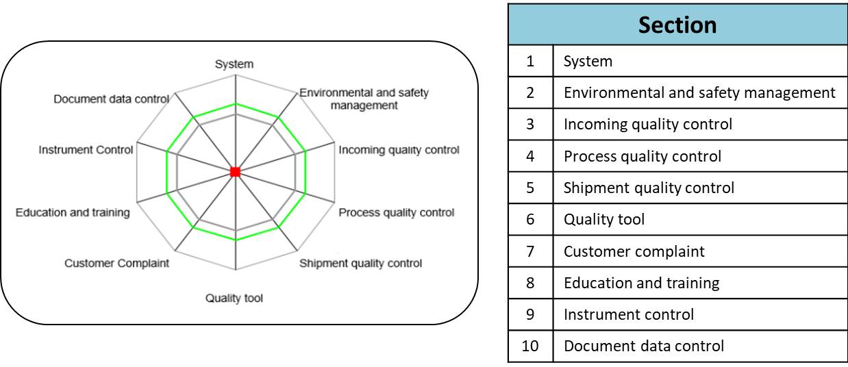
I. The auditing of new supplier qualifications is divided into the system audit and the production process audit
System audit: system, environmental and safety management, incoming quality control, process quality control, shipment quality control, quality tool, customer complaint, education and training, instrument control, and document data control.
Production process audit: solder paste management, stencil management, ESD management, rework management, SFCS management, SMT process management, and warehouse management.
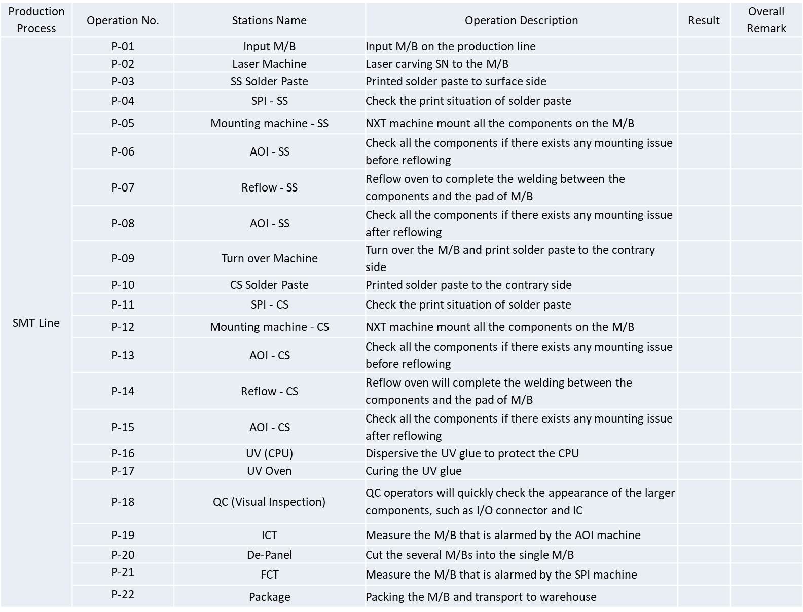
II. SMT IPQC daily evaluation chart
Safeguarding the process quality of every procedure:
III. Increase SMT yield rate
- SMT on-site audit
- OQC inspection
- Weekly meetings with suppliers and audits of weekly SMT quality reports
- Problem analysis will be conducted with the suppliers with follow-up enhancement being tracked
IV. Analysis of common SMT problems, such as poor solder, shift, missing component, tombstone, and side up
| Possible causes of poor solder | Environment | Temperature | Humidity | Dust | Ventilation | Other | |
| Staff | Solder paste preservation problem | Uneven solder | Gesture operation | Solder insufficiency | Shift | Other | |
| Processing method | Incorrect feeding method | Insufficient solder paste stirring | Scraper deformation | Inappropriate choice of solder paste | Wrong shape of the steel plate opening | Other | |
| Machine | Printing speed too fast/slow | Wrong speed/temperature of reflow oven | Poor solder paste printing | Uncleanness of steel plate | Inappropriate solder paste machine gap | Other | |
| Material | Dampened | Uneven thickness | Re-usage of consumables | Poor inventory condition | Uneven PCB | Other |
| Wrong position or shift of the component | Environment | Environmental humidity not meeting the requirement | Air flow too fast | Room temperature too high | Solder paste hardening after printing | Exposed to the air for too long after PCB printing | |
| Staff | Manual loading | Tin shortage | Board hit or pushed by hand | PCB collision in the reflow oven not noticed in QC | Other | ||
| Processing method | Not following the SOP | Exhaust speed of reflow oven too fast | Inappropriate thickness of solder paste | Inappropriate size of steel plate aperture | Reflow oven temperature too high | Other | |
| Machine | Bad vacuum | Wrong coordinates | Poor rack | Worn nozzle | Nozzle too small | Other | |
| Material | Part oxidation | Deformation of rejected item | Solder paste deterioration | PCB oxidation | Incoming damaged | Other |
| Tombstone | Environment | Excessively humid | Too dusty | Temperature too high | Poor ventilation | Other | |
| Staff | Uneven thickness of handprints | Shifting of manually placed parts | Addition of solder paste is too slow | Uneven solder | 軌道未及時清理
Track not cleaned up in time |
Other | |
| Processing method | Stacking time too long | Insufficient gap between parts | Wrong incoming method | Coordinates wrongly modified | Mix use of new and old solder paste | Other | |
| Machine | Power failure | Clutter in the reflow oven | Deformation/poor angle of the solder paste machine scraper | Solder paste on the tracks | Deviation of loading | Other | |
| Material | Dust-free cloth napping | Internal gap of the PAD is too big | Inconsistency of the component and the PAD | Poor solder paste compatibility of the PAD | Uneven thickness of the parts | Other |
| Side up | Environment | Fast volatilization of Solder paste | Ventilation | Other | |||
| Staff | Pull test of parts | Man-made damage/collision | Insufficient materials | Solder paste wiped with hand | Manual packaging of loose materials | Other | |
| Processing method | Uneven heating of PCB | Poot PCB design | Incomplete SOP | Manual placement of loose material | Expired solder paste | Other | |
| Machine | Part Data | Inappropriate temperature of reflow oven | Uneven printing of solder paste | Placement pressure too big | Shifting of coordinates | Other | |
| Material | Part oxidation | Inappropriate packaging of parts | PAD oxidation | Inappropriate distance of PAD | PCB benching | Other |
Allion offers three major SMT services exclusive to our customers
- Rigorous scientific-based methods: Scientific working methods and procedures are applied to any unexpected incidents in the factory, as the problem is carefully analyzed and resolved step by step. We insist on using data to comprehend facts and solve problems with scientific approaches. We institute our faith in quality enhancement, consumption reduction, and economic benefit enhancements. Allion is always striving to achieve more enhancements for its professional skills and core capability to inspire further proactivity and creativity.
- To satisfy customers’ demands and offer the required technical support, earning customers’ trust in our ability to fulfill all of their needs, from the evaluation of the ODM factory quality, product development, order acceptance, material procurement, incoming audits, production process control, and shipment, to the after-sales services, with our close cooperation with the ODM/vendors, every step of the procedure will be carried out in the specific way required by the customers.
- The quality control of the whole SMT process requires professional systemic engineering. To achieve stable production quality, Allion utilizes systemic thoughts, design, and control of the engineering design, choice of materials, and on-site process. The purpose of control is to comprehensively fulfill the process requirement and maintain the stability of process quality. In addition to mastering the SMT process (method, requirement, and key process technologies), engineering know-how, as well as the mechanism and correct response to general poor soldering issues, we will also establish an effective quality control system to swiftly solve all production process problems at once.
In the next article, Allion releases the most valuable content for everyone—our first-hand factory problem analysis. Stay tuned to our newsroom and LinkedIn for the latest updates.
Take the Next Step
If you‘re searching for ways to improve your product, the team at Allion can help! From product design to device debugging, we have the industry knowhow to assist you through the entire product lifecycle. Feel free to email us directly or schedule a consultation today.